ATmega644P/ATmega1284P Notes
- 64K/128K Flash program memory
- 4K/16K SRAM
- 2K/4K EEPROM
- Two 8-bit Timer/Counters
- One/Two 16-bit Timer/Counter
- Six PWM Channels
- Eight channel 10-bit ADC
- Two Serial USARTs
- One Master/Slave SPI Serial Interface
- One 2-wire Serial Interface (Philips I2C compatible)
With a 16 MHz clock, clockCyclesPerMicrosecond() is
16000000 / 1000000 or 16 clock cycles per microsecond,
a 20 MHz clock gives 20/msec.
- TIMER0 is 8-bit
used by millis() and micros()
programmed for 4 µs per count.
- TIMER1 is 16-bit
- TIMER2 is 8-bit
- TIMER3 is 16-bit (ATmega1284P only)
- USART0 (can be used as an SPI master bus)
- USART1 (can be used as an SPI master bus)
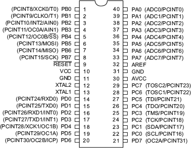
- PCINT0 on d31
- PCINT1 on d30
- PCINT2 on d29
- PCINT3 on d28
- PCINT4 on d27
- PCINT5 on d26
- PCINT6 on d25
- PCINT7 on d24
- PCINT8 on d0
- PCINT9 on d1
- PCINT10/IINT2 on d2
- PCINT11 on d3
- PCINT12 on d4 (SS)
- PCINT13 on d5 (MOSI)
- PCINT14 on d6 (MISO)
- PCINT15 on d7 (SCK)
- PCINT16 on d16 (SCL)
- PCINT17 on d17 (SDA)
- PCINT18 on d18 (TCK)
- PCINT19 on d19 (TMS)
- PCINT20 on d20 (TDO)
- PCINT21 on d21 (TDI)
- PCINT22 on d22
- PCINT23 on d23
- PCINT24 on d8 (RXD0)
- PCINT25 on d9 (TX0)
- PCINT26/INT0 on d10 (RXD1)
- PCINT27/INT1 on d11 (TXD1)
- PCINT28 on d12
- PCINT29 on d13
- PCINT30 on d14 (ICP1)
- PCINT31 on d15
ATmega644P/ATmega1284P
| General |
| Physical |
Logical |
Function |
Description |
| 9 |
|
RESET |
|
| 10 |
|
VCC |
+5V |
| 11 |
|
GND |
|
| 12 |
|
XTAL2 |
|
| 13 |
|
XTAL1 |
|
| 30 |
|
AVCC |
+5V |
| 31 |
|
AGND |
|
| 32 |
|
AREF |
|
| Port A |
| Physical |
Logical |
Function |
Description |
| 33 |
d24 |
a7 |
|
| 34 |
d25 |
a6 |
|
| 35 |
d26 |
a5 |
|
| 36 |
d27 |
a4 |
|
| 37 |
d28 |
a3 |
|
| 38 |
d29 |
a2 |
|
| 39 |
d30 |
a1 |
|
| 40 |
d31 |
a0 |
|
| Port B |
| Physical |
Logical |
Function |
Description |
| 1 |
d0 |
|
|
| 2 |
d1 |
|
|
| 3 |
d2 |
INT2 |
|
| 4 |
d3 |
|
|
| 5 |
d4 |
SS |
SPI |
| 6 |
d5 |
MOSI |
SPI |
| 7 |
d6 |
MISO |
SPI |
| 8 |
d7 |
SCK |
SPI |
| Port C |
| Physical |
Logical |
Function |
Description |
| 22 |
d16 |
SCL |
TWI |
| 23 |
d17 |
SDA |
TWI |
| 24 |
d18 |
TCK |
JTAG |
| 25 |
d19 |
TMS |
JTAG |
| 26 |
d20 |
TDO |
JTAG |
| 27 |
d21 |
TDI |
JTAG |
| 28 |
d22 |
|
|
| 29 |
d23 |
|
|
| Port D |
| Physical |
Logical |
Function |
Description |
| 14 |
d8 |
RXD0 |
USART |
| 15 |
d9 |
TXD0 |
USART |
| 16 |
d10 |
RXD1 |
USART |
| 17 |
d11 |
TXD1 |
USART |
| 18 |
d12 |
|
|
| 19 |
d13 |
|
|
| 20 |
d14 |
ICP1 |
|
| 21 |
d15 |
|
|
Copyright © 2011, 2012, 2014, 2015, 2017, 2018, 2019, 2020, 2021
Craig Leres